
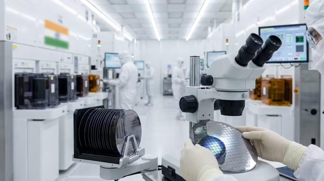


India semiconductor manufacturing is entering a new phase, with artificial intelligence at its centre. AI is driving demand for chips, and it is also changing how chips are designed, made, tested and packaged. India wants a share of both sides of that change: more chips made in the country, and more of the tools that make chipmaking possible. Semicon India 2.0, approved in July 2026 with an outlay of Rs 1,27,500 crore, covers chip design, equipment and materials, fabrication, advanced packaging, research and skills.
The first phase of the Semicon India Programme, backed by Rs 76,000 crore, concentrated on attracting manufacturing investment. By September 2026, five of the 12 approved units were in commercial production, and more than 105 chip-design startups had access to industry-grade Electronic Design Automation tools. Those are useful foundations, but a gap remains between using imported engineering tools and building products domestic firms can own and sell. India semiconductor manufacturing can use AI to narrow that gap.
India semiconductor manufacturing: where AI fits in design
Chip designers juggle performance, power, heat and cost, and AI can help by exploring the options and shortening key design tasks. Google has used an AI method to place components on a chip and says it has applied it to its last three generations of AI processors. India semiconductor manufacturing can build on a real strength here. The country holds nearly 20 percent of the world’s chip design workforce, with about 125,000 chip-design engineers, most of them in multinationals’ design centres in Bengaluru. The Chips to Startup programme has trained around 70,000 more. The next step could be moving from using tools to building them, and Semicon 2.0, which aims to support at least 200 chip-design companies, could give the tools their first users.
Fabs operate under precision, where small variations in equipment, temperature or materials can cut yield. AI can analyse manufacturing data to spot defect patterns, anticipate equipment failures and help optimise production settings. It can warn that a machine is likely to fail. A sensor detecting a rise in a machine’s temperature could trigger maintenance before a batch is spoiled. The Tata Electronics and Powerchip fab at Dholera in Gujarat, due to begin commercial operations in mid-2028, could serve as a testing place for India semiconductor manufacturing, since the plant will use data analytics and machine learning.
Inspection, testing and packaging
AI-powered vision systems can spot defects that conventional inspections miss. A July 2026 survey reported 98 to 99 percent accuracy in certain semiconductor manufacturing tasks, but only 17 percent of the systems reviewed had reached high-volume manufacturing, held back by false positives, inconsistent data labelling and declining performance as conditions changed. This gap could open a door for India. As scaling an inspection system can only be proven on a live line, India’s assembly and test units can serve as a proving ground for AI inspection tools. India semiconductor manufacturing needs that kind of proof before buyers will trust home-grown tools.
Packaging and testing can build manufacturing expertise while wafer fabrication matures. Advanced packaging combines multiple chips in compact arrangements, making thermal management and quality control increasingly important. AI can support these processes by analysing manufacturing data and improving thermal modelling to predict heat flow. A model trained on past test results could flag packages likely to overheat before they ship. Nine of the 12 projects approved under the India Semiconductor Mission are packaging units, including Micron’s facility at Sanand in Gujarat, which began production in February 2026. India semiconductor manufacturing can build expertise through packaging while fabrication matures.
India semiconductor manufacturing and the talent gap
None of this works without people to run the factories. The National Institute of Electronics and Information Technology Calicut’s training lab is training over 100,000 engineers. A partnership between the India Semiconductor Mission, the Indian Institute of Science and Lam Research aims to train 60,000 people. India semiconductor manufacturing also needs computing power. The India AI Mission, budgeted at about Rs 10,372 crore, has pushed shared GPU capacity past 45,000 as of June 2026, and 20 Indian foundation model proposals were chosen from 506. Data centre capacity has grown from 375 MW in 2020 to about 1,575 MW.
Three priorities could turn investment into capability. India needs domestic industrial AI solutions, built by its IT services and deep-tech firms with fabs and packaging units and global equipment vendors. It needs industry-linked testbeds where manufacturers, universities and startups test AI tools against real production problems, starting with predictive maintenance and defect detection. And it needs specialised semiconductor engineering and technical training, with universities, research institutions and industry together building expertise. The India AI Impact Summit in February 2026 drew over 100 countries. India semiconductor manufacturing will be judged on whether those plans turn into factories, tools and jobs.