
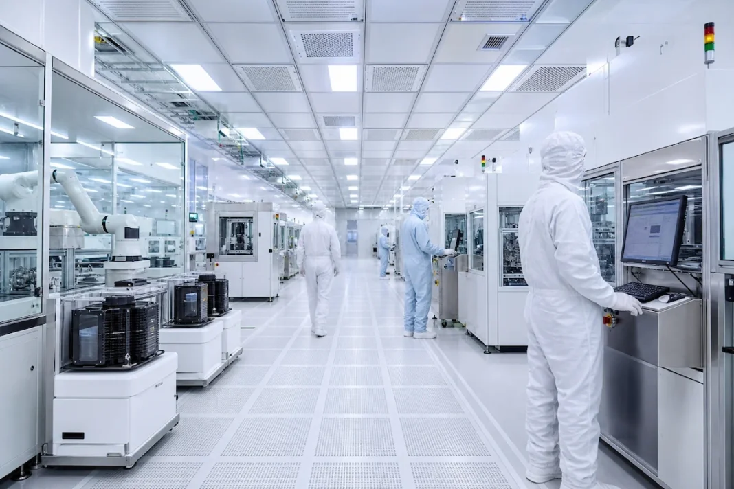


HCLTech Rapidus work on 2-nanometer logic chips took a formal step forward on 26 October 2026, when Rapidus and HCL Technologies signed an engineering partnership at HCLTech headquarters in Noida. East Asia Brief reported on 1 November 2026 that the agreement sets up two dedicated engineering centres in Bengaluru and Hubli to support chip manufacturing at Rapidus. The centres began commercial operations the same day the agreement was signed, and joint design work was expanded through 30 October.
Rapidus is a Japanese foundry building its first fabrication plant, Innovative Integration for Manufacturing, in Chitose, Hokkaido. It aims to begin commercial mass production of 2-nanometer logic chips in fiscal 2027. The HCLTech Rapidus centres in India are meant to close a design talent gap in Japan, where domestic universities produce fewer specialised device engineers than cutting-edge logic production needs, after three decades of foundry market share losses.
HCLTech Rapidus centres in Bengaluru and Hubli
The HCLTech Rapidus centres will build process design kits, the software packages that carry design rules and simulation models for manufacturing. Rapidus plans to release those kits during fiscal 2026 to prospective semiconductor customers. Engineers at the sites will also handle design technology co-optimisation, the simultaneous tuning of circuit layout and fabrication steps, which reduces defect rates before silicon runs begin in Japan.
The scope of the HCLTech Rapidus work spans mask design, design infrastructure and physical layout design. Those operations verify that electronic circuits translate accurately onto optical masks used in extreme ultraviolet lithography tools. Hubli was picked alongside Bengaluru to tap engineering talent outside India’s main tech hubs, and the two centres run on synchronised networks to mirror Tokyo operational hours. Neither company disclosed the contract value or the capital spending allocated to the two centres, and the number of engineers assigned to them was also withheld, according to exchange filings in Mumbai.
HCLTech Rapidus talent pipeline
The HCLTech Rapidus partnership sets up a talent pipeline to recruit and train Indian engineering graduates. Selected engineers will relocate to Japan to add to the technical workforce at Rapidus facilities, Rapidus chief executive Atsuyoshi Koike said at the signing. HCL Technologies chief executive C Vijayakumar signed the agreement with Koike in Noida. The pipeline is a direct answer to Japan’s shortage of semiconductor design engineers, and it gives Indian graduates a route into work on 2-nanometer production.
The agreement follows the launch of Rapidus CORE on 5 October 2026, a framework Rapidus set up with 17 initial design partners to build an intellectual property and design service network. HCL Technologies joined that programme as an official Design Solution Alliance partner. The Indian IT company has similar design partnerships with Taiwan Semiconductor Manufacturing Co., Samsung Electronics and Intel, and it has completed more than 230 tape-outs across global foundries. It also runs a 40,000-square-foot testing and silicon validation cleanroom at its main campus in Bengaluru.
HCLTech Rapidus and the wider chip race
Foundries need mature design service networks so fabless customers can move chip architectures onto a new manufacturing process without long delays. Without third-party design houses, fabless clients cannot access proprietary manufacturing recipes at reasonable cost. Rapidus runs a model designed to shorten production cycle times for custom artificial intelligence processors, and that model needs fast translation from customer architectural files into ready masks. The HCLTech Rapidus centres supply that design capacity from India.
IBM Japan opened a dedicated technical office in Chitose on 26 October to assist local operations. IBM licensed the baseline 2-nanometer nanosheet transistor architecture to Rapidus under a 2022 bilateral research pact. The Japanese government has approved 920 billion yen, about $6 billion, in subsidies for Rapidus through the Ministry of Economy, Trade and Industry, to fund cleanroom construction and equipment installation in Hokkaido. India has sought closer semiconductor ties with Japan under bilateral supply chain agreements signed in 2023, with India promoting domestic chip design while Japanese foundries supply advanced manufacturing capacity.
Rapidus plans to distribute its 2-nanometer process design kits to selected customers in fiscal 2026, while commercial wafer output remains scheduled to start in Chitose during fiscal 2027. The regulatory filings do not state the financial value of the contract, the capital spending for the two centres, or the total headcount for the talent pipeline.